GFET-S10 for Sensing applications
In stock
Overview
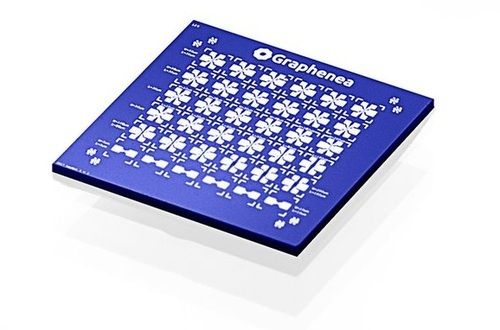
GFET-S10 (Die size 10 mm x 10 mm) - Processed in Clean Room Class 1000
Growth method: CVD synthesis
· Polymer assisted transfer
· Chip dimensions: 10 mm x 10 mm
· Chip thickness: 675 μm
· Number of GFETs per chip: 36
· Gate oxide thickness: 90 nm
· Gate oxide material: SiO2
· Dielectric Constant of the SiO2 layer: 3.9
· Resistivity of substrate: 1-10 Ω.cm
| Product Code | GFET-S10 :pack of 4 |
|---|---|
| Brand | Ultrananotech |
| Usually dispatched in | 2-3 weeks |
| Pack Size | pack of 4 |